And Gate
3-state 2-input AND gate with Schmitt-trigger inputs and ESD-protected UART ports for the PomeLabs Core Kit.
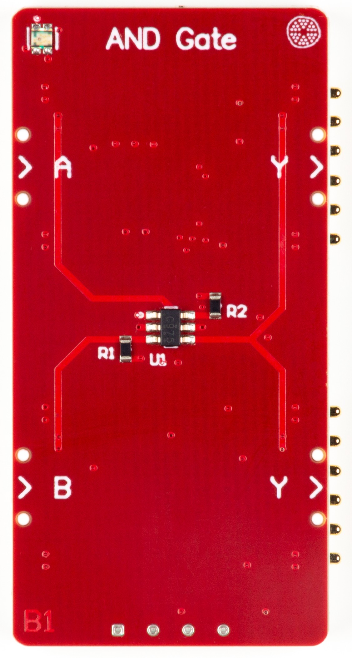
The PomeLabs AND Gate Module (PML-AG-01) makes Boolean logic tangible. Wire two signals in, observe a HIGH output only when both are HIGH — and do it on hardware that is Schmitt-trigger hardened, input tolerant, and ESD-protected on all four UART ports. The underlying IC can implement nine different logic functions; this module is configured and verified for AND.
Revision: v1.0 | Part Number: PML-AG-01 | Series: PomeLabs Core Kit
Pinout

Schematic

Digital Twin
In the PomeLabs App, the PML-AG-01 is mirrored as a digital twin in both the Playground and inside any Connect Activity. Drive both inputs from the App's signal controls and watch the output respond in real time — or observe the physical output on the module while the App streams back the live logic state.
Controls — parameters you can set from the App
Logic input A · pin S+_UL · toggle, HIGH / LOW
Drives the first AND gate input. Set HIGH or LOW from the App to step through the truth table.
Logic input B · pin S+_LL · toggle, HIGH / LOW
Drives the second AND gate input. Combine with input A to explore all four input combinations.
UART TX — Upper-Left / Lower-Left · pins TX_UL-L, TX_LL-L · serial data source
Drives USART1/USART3 transmit lines through D1/D3 ESD protection.
UART TX — Upper-Right / Lower-Right · pins TX_UR-L, TX_LR-L · serial data source
Drives USART2/USART4 transmit lines through D2/D4 ESD protection.
Monitors — values streamed back from the module
Gate output Y · pins S+_UR / S+_LR · digital indicator, HIGH / LOW
Live AND gate output. HIGH only when both inputs A and B are HIGH. Updates in real time as inputs change.
UART RX — all four ports · serial data traces
Inbound data from downstream nodes through D1–D4 ESD protection back to the Backend MCU.
Datasheet
1. Overview
The PML-AG-01 implements a 2-input AND gate using the SN74LVC1G99DCUR (U1) — Texas Instruments' ultra-configurable single-gate device capable of nine logic functions in one package. On this module, configuration pins C and D are hard-tied to GND (L) on the PCB, and OE is hard-tied to GND, permanently selecting the 3-state 2-input AND function.
When both inputs A (S+_UL) and B (S+_LL) are HIGH, output Y (S+_UR and S+_LR) is HIGH. Any other input combination produces a LOW output. The Schmitt-trigger input stage ( hysteresis typ at = ) ensures clean transitions even with slow or noisy input signals — a critical property in educational environments where signal sources may not be ideal. Four USBLC6-2P6 ESD protection devices (D1–D4) protect all four UART ports.
2. BOM Components
| Ref. | Type | Value / Part | Role on this module |
|---|---|---|---|
| U1 | Configurable logic gate | SN74LVC1G99DCUR (TI) | Configured as 3-state 2-input AND: C = D = GND, OE = GND. Schmitt-trigger inputs ( hysteresis typ at = ). VSSOP-8 (DCU) package, . |
| D1 | ESD protection IC | USBLC6-2P6 (ST) | IEC 61000-4-2 Level 4 ESD clamp on Upper-Left UART port. max. SOT-666. |
| D2 | ESD protection IC | USBLC6-2P6 (ST) | IEC 61000-4-2 Level 4 ESD clamp on Upper-Right UART port. Identical to D1. |
| D3 | ESD protection IC | USBLC6-2P6 (ST) | IEC 61000-4-2 Level 4 ESD clamp on Lower-Left UART port. Identical to D1. |
| D4 | ESD protection IC | USBLC6-2P6 (ST) | IEC 61000-4-2 Level 4 ESD clamp on Lower-Right UART port. Identical to D1. |
| R1, R2 | Resistor | Pull-up resistors on UART TX/RX lines to 3V3. | |
| p1–p4 | Connector | Node headers | Four node connectors exposing +5V, GND, S+, S−, RX/TX, TX/RX to downstream modules. |
3. Electrical Specifications
All values at unless otherwise noted. Gate specifications from TI SCES609G (SN74LVC1G99, Rev. G, Nov 2013). ESD protection from ST DS4260 Rev. 7 (USBLC6-2P6, Dec 2021).
3.1 U1 — SN74LVC1G99DCUR
The SN74LVC1G99 features configurable multiple functions with a 3-state output. The output is disabled when the output-enable (OE) input is HIGH. When OE is LOW, the output state is determined by 16 patterns of the 4-bit input (A, B, C, D). Selectable functions include MUX, AND, OR, NAND, NOR, XOR, XNOR, inverter, and buffer. All inputs can be connected to or GND.
3.1.1 Absolute Maximum Ratings
Exceeding these values may permanently damage the device. Stress ratings only.
| Parameter | Max Value | Unit |
|---|---|---|
| Supply voltage () | to | V |
| Input voltage () | to | V |
| Output voltage — high-Z or power-off state () | to | V |
| Output voltage — high or low state () | to | V |
| Input clamp current (), | mA | |
| Output clamp current (), | mA | |
| Continuous output current () | mA | |
| Continuous current through or GND | mA | |
| Package thermal impedance () — DCU package | °C/W | |
| Storage temperature () | to | °C |
3.1.2 Recommended Operating Conditions
| Parameter | Min | Max | Unit / Notes |
|---|---|---|---|
| Supply voltage () — operating | V | ||
| Supply voltage () — data retention only | — | V | |
| Input voltage () | V — inputs accept up to regardless of | ||
| Output voltage () | V | ||
| High-level output current () @ = | — | mA — sourcing | |
| Low-level output current () @ = | — | mA — sinking | |
| High-level output current () @ = | — | mA — sourcing | |
| Low-level output current () @ = | — | mA — sinking | |
| Input transition rise/fall rate () @ = | — | ns/V | |
| Operating temperature () | °C |
3.1.3 Electrical Characteristics
| Parameter | Typical | Max | Condition |
|---|---|---|---|
| Positive-going input threshold () | — | = — Schmitt trigger | |
| Negative-going input threshold () | — | = | |
| Input hysteresis () | = | ||
| Propagation delay () A/B → Y | — | = , = | |
| Propagation delay () C → Y | — | = , = | |
| Propagation delay () D → Y | — | = , = | |
| Propagation delay () A/B → Y | — | = , = | |
| Output enable time () | — | = , = | |
| Output disable time () | — | = , = | |
| Quiescent supply current () | — | = or GND, = | |
| Input capacitance () | — | = | |
| Output capacitance () | — | = | |
| Power dissipation capacitance () | — | = , = |
4. Truth Table
On this module, OE, C, and D are hard-tied LOW on the PCB — selecting the 3-state 2-input AND function. The output is therefore determined entirely by inputs A and B:
| OE | A (S+_UL) | B (S+_LL) | C (tied L) | D (tied L) | Y Output |
|---|---|---|---|---|---|
| L | L | L | L | L | L — output LOW |
| L | L | H | L | L | L — output LOW |
| L | H | L | L | L | L — output LOW |
| L | H | H | L | L | H — AND true |
The high-impedance state (Y = Z) is not reachable on this module because OE is hardwired LOW.
5. Logic Function Configuration Reference
The SN74LVC1G99 supports nine distinct logic functions selected by the static levels on A, B, C, D, and OE. The table below shows common configurations for reference — only the AND configuration is wired on this PCB.
| Function | OE | A | B | C | D |
|---|---|---|---|---|---|
| 3-state 2-input AND (this module) | L | Input 1 | Input 2 | L | L |
| 3-state 2-input NAND | L | Input 1 | Input 2 | H | L |
| 3-state 2-input OR | L | Input 1 | H | Input 2 | L |
| 3-state 2-input NOR | L | Input 1 | H | Input 2 | H |
| 3-state 2-input XOR | L | Input 1 | L | Input 2 | H |
| 3-state 2-input XNOR | L | H | L | Input 1 | Input 2 |
| 3-state buffer | L | Input | H or L | L | L |
| 3-state inverter (NOT) | L | Input | H or L | L | H |
| Output disabled (high-Z) | H | X | X | X | X |
6. Pin Descriptions
All signal pins are referenced to GND.
| Pin / Net Name | Direction | Description |
|---|---|---|
| S+_UL | Input | Logic input A to U1. Upper-Left signal — first AND gate input. |
| S+_LL | Input | Logic input B to U1. Lower-Left signal — second AND gate input. |
| S+_UR / S+_LR | Output | AND gate output Y. HIGH only when both A and B are HIGH (OE is hardwired LOW). Drives both output channels simultaneously. |
| TX_UL-L / TX_LL-L | Input | UART transmit from Backend MCU (USART1/USART3). Through D1/D3 ESD protection. |
| RX_UL-L / RX_LL-L | Output | UART receive from Upper-Left and Lower-Left connectors. Through D1/D3 ESD protection. |
| TX_UR-L / TX_LR-L | Input | UART transmit from Backend MCU (USART2/USART4). Through D2/D4 ESD protection. |
| RX_UR-L / RX_LR-L | Output | UART receive from Upper-Right and Lower-Right connectors. Through D2/D4 ESD protection. |
| 5V-Module | Power In | supply. Powers of U1 and VBUS of D1–D4. |
| 3V3 | Power In | logic rail for pull-up resistors R1–R2 (). |
| GND | Ground | Common ground for all ICs and connectors. |
7. Connection Guide & Common Errors
Correct power-up sequence:
- Connect GND first, shared across all modules on the common bus.
- Connect 5V-Module to a regulated source to power U1 and the VBUS pins of D1–D4.
- Connect the 3V3 rail for the UART pull-up resistors.
- Apply logic signals to S+_UL (A) and S+_LL (B). The output appears immediately on S+_UR / S+_LR — there is no enable step because OE is hardwired LOW on the PCB.
Logic-level reference (Schmitt-trigger inputs): at = , an input must rise above to register as HIGH and fall below to register as LOW. Signals stuck inside the hysteresis band (–) hold the previous logic state — useful for noise immunity, but worth knowing when probing slow analog-like signals.
Common wiring errors and consequences:
| Mistake | Symptom | Correction |
|---|---|---|
| to U1 exceeds | U1 permanently damaged (absolute max ) | Keep 5V-Module rail . |
| Input signal on S+_UL or S+_LL exceeds | Input clamp current flows; permanent damage if exceeds | Inputs are tolerant — never exceed it. Add a series resistor if your source can swing higher. |
| Output Y driving load | Continuous output current absolute max exceeded — U1 may overheat or fail | Keep total on the Y output (across S+_UR + S+_LR) within absolute max. For sustained operation, design for at or at . |
| Input signal with very slow edges (slower than at ) | Operation outside guaranteed input transition rate; Schmitt-trigger hysteresis improves robustness but TI does not specify behavior | Buffer slow signals with another logic stage if reliability is critical. |
| USBLC6-2P6 VBUS pin on D1–D4 unconnected | ESD protection ineffective — UART pins exposed to direct ESD strikes | Ensure 5V-Module is connected; it powers VBUS of all four ESD ICs. |
| Powering inputs while 5V-Module is OFF | circuitry isolates U1 and prevents back-drive damage — designed-in safe condition, not a fault | No action needed; this is supported behavior of the device. |
Note: OE, C, and D are hard-tied to GND on the PCB and are not user-accessible. The common floating-input mistakes that apply to bare SN74LVC1G99 designs (floating OE → high-Z output; floating C/D → undefined function) do not apply to this assembled module.
Hands-on Labs
Get started with the PML-AG-01 through guided labs that build from truth table verification to timing analysis and gate combinations. Each lab opens in the PomeLabs app.
And Gate Onboarding
Power up the module, step through all four input combinations, and verify the truth table on the output. Recommended starting point.
Schmitt Trigger Inputs
Apply slow-rising and noisy input signals and observe how the Schmitt-trigger hysteresis produces clean output transitions.
Propagation Delay Measurement
Drive the AND gate with a fast input signal and measure the input-to-output propagation delay on an oscilloscope. Compare against the $7.5\,\mathrm{ns}$ max spec at $3.3\,\mathrm{V}$.
Combinational Logic Circuits
Combine the AND Gate module with OR, NOT, and other gate modules to build and verify more complex Boolean logic expressions.
Use Cases
Coming soon.
How is this guide?